“TSMC Charts the Future of AI: A Trillion-Dollar Silicon Economy Driven by A13 and Wafer-Scale Packaging”
- ashley19241
- 9 hours ago
- 5 min read

At TSMC's 2026 Technology Symposium, the most striking opening message was not merely about process node scaling, but a bold outlook on the broader market: driven by advanced semiconductor technologies, the industry is now expected to reach the long-anticipated US$1 trillion milestone—originally projected for 2030—as early as this year.
As artificial intelligence rapidly evolves from generative AI to agentic AI and further into physical AI, the technology landscape is undergoing a profound transformation. At this year's forum, TSMC not only unveiled its next-generation process roadmap, including A14 and A13 nodes, but also introduced its SoW-X wafer-level packaging technology, which exceeds 40 times the reticle size.
Through these technological advancements, we gain not only deeper insight into TSMC's leadership in semiconductor manufacturing, but also a clearer view of the trajectory shaping the AI and semiconductor markets in the years ahead.
Advanced Logic Processes: A14 Targets Key Customers, A13 Strengthens Seamless Technology Transition
In advancing leading-edge process technologies, TSMC continues to maintain a disciplined and steady cadence. According to the latest technology roadmap released at the event, the N2 process successfully entered mass production in the fourth quarter of 2025.
Meanwhile, the highly anticipated A16 process—featuring Super Power Rail (SPR) technology—is expected to reach production readiness in the second half of this year.

Toward the Angstrom Era: TSMC Unveils Its Roadmap
Looking ahead to the Angstrom era, TSMC further outlined its detailed roadmap:
A14 Process (2nd-Generation Nanosheet Transistors):Scheduled to enter mass production in 2028 as planned.
A14 adopts TSMC's NanoFlex Pro technology. Compared with the N2 process, it delivers up to a 15% speed improvement at the same power consumption, or up to a 30% power reduction at the same performance level.
TSMC emphasized that all major industry players have shown strong interest in adopting the A14 process.
A13 Process Debut: Expected to enter production in 2029, one year after A14 reaches mass production.
A13 is a direct shrink of the A14 process, enabling customers to seamlessly migrate their existing A14 designs. Compared to A14, A13 achieves an additional 6% reduction in die area, along with further improvements in power efficiency and performance.
Beyond Nanosheet: Next-Generation Technology
For post-nanosheet technologies, TSMC showcased the world’s smallest functional 6T SRAM CFET (Complementary Field-Effect Transistor) memory cell. Its layout area is approximately 30% smaller than conventional nanosheet-based designs.
Market Implications
For IC design leaders such as NVIDIA, AMD, Apple, and Qualcomm, redesigning chip architectures at nodes below 2nm involves astronomical R&D and mask costs.
TSMC's backward-compatible strategy with A13 provides a low-friction, high return-on-investment upgrade path, significantly increasing customer stickiness among top-tier clients. This approach also makes it considerably more difficult for competitors—such as Intel and Samsung—to displace existing customers at more advanced process nodes.
Packaging as a System: CoWoS Scales Up, SoW-X Breaks Physical Limits
If advanced logic processes are the heart of AI computing power, then advanced packaging serves as the structural framework that determines the scale of these AI giants.
This year, TSMC announced the production of the world's largest CoWoS package at 5.5 times the reticle size, while achieving an impressive yield rate exceeding 98%. However, this is only the beginning:
By 2028, TSMC is expected to mass-produce 14× reticle-size CoWoS, capable of integrating up to 20 HBM (High Bandwidth Memory) stacks. By 2029, CoWoS will exceed the 14× reticle size and is projected to support up to 24 HBM stacks.
The Game Changer: TSMC-SoW Technology
An even more disruptive innovation is TSMC's System-on-Wafer (TSMC-SoW) technology. The current SoW-P, designed for logic die integration, has already entered mass production in 2024. Meanwhile, the more advanced SoW-X, which integrates both logic and HBM dies, is expected to reach production readiness by 2029.
SoW-X will expand the interposer size to over 40 times the reticle size, enabling integration of up to 64 HBM stacks and 16 compute dies. This breakthrough is designed to meet the rapidly growing demand for next-generation AI computing at unprecedented scale.
Market Implications
The emergence of SoW-X effectively signals the full arrival of the “system-on-wafer” era. As generative AI and large language models continue to scale exponentially in parameter size, relying solely on Moore's Law-driven transistor scaling is no longer sufficient to meet the massive demands for memory bandwidth and data throughput.
For cloud service providers (CSPs) actively building hyperscale computing clusters, SoW-X is expected to become a critical infrastructure enabler for achieving next-generation artificial general intelligence (AGI).
At this stage, TSMC's technological “moat” built around 3D Fabric and advanced packaging appears even more difficult to overcome than its leadership in advanced logic process technologies.
Silicon Photonics COUPE: Unlocking AI Compute Potential
As computing power and chip sizes continue to surge, data transmission energy consumption and latency have become critical bottlenecks to overall system performance.
To address this challenge, TSMC is actively advancing its Compact Universal Photonic Engine (COUPE) technology.
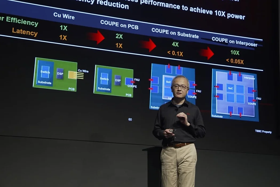
According to TSMC, the world's first 200Gbps micro-ring modulator (MRM) powered by COUPE technology is expected to enter mass production this year.
Looking ahead, TSMC aims to further expand performance through technologies such as wavelength multiplexing, targeting an ultra-high bandwidth density of 4 Tbps/mm by 2030.
Conclusion: Dual Growth Engines and a Commitment to Sustainability
Based on market data and capacity outlook, high-performance computing (HPC) and artificial intelligence (AI) have already accounted for 55% of the overall semiconductor market.
Looking ahead, TSMC's future growth engines are clearly centered on these two key sectors.

To meet this seemingly insatiable demand, TSMC is undergoing an unprecedented expansion:
From 2022 to 2026, customer demand for AI accelerators is expected to grow by as much as 11 times.
For AI-critical advanced packaging technologies such as CoWoS and SoIC, capacity is projected to achieve a compound annual growth rate (CAGR) exceeding 80% between 2022 and 2027.
Capacity for the most advanced nodes, including N2 and A16, is expected to deliver a 70% CAGR from 2026 to 2028.
Beyond rapid advances in technology and capacity, TSMC also emphasizes its commitment to sustainability as a global corporate citizen. The company has pledged to follow Science-Based Targets (SBTs), aiming to achieve net-zero emissions by 2050.
At this year's technology forum, TSMC also introduced its first-ever ESG-themed pavilion, showcasing collaborative innovations with customers focused on low power consumption and high energy efficiency.

Final Summary:
Overall, TSMC's 2026 Technology Symposium was not merely a full-scale showcase of cutting-edge innovations, but also a forward-looking blueprint outlining the trajectory of AI hardware development over the next decade.
From the seamless scaling enabled by A13, to the ultimate wafer-level integration of SoW-X, and the strategic deployment of silicon photonics through COUPE, TSMC is leveraging a three-pronged approach—advanced logic processes, advanced packaging, and optoelectronic integration—to firmly anchor the world's leading AI players within its ecosystem.
With the global silicon economy projected to reach US$1.5 trillion by 2030, TSMC appears well-positioned to secure the largest share of this rapidly expanding market.
<Originally published by partner media outlet mashdigi and republished with permission by United Daily News.>
Source of Information: Tech UDN


Comments